- 您现在的位置:买卖IC网 > Sheet目录341 > MAX8821ETI+ (Maxim Integrated)IC LED DRVR WHITE BCKLGT 28-TQFN
�� �
�
�White� LED� Charge� Pump� with� Mono� Class� D�
�Audio� Amp� and� Dual� LDO�
�Audio� Amplifier�
�The� audio� amplifier� in� the� MAX8821� is� a� 2W� Class� D�
�loudspeaker� amplifier.� The� amplifier� features� a� low-�
�power� shutdown� mode� and� industry-leading� click-and-�
�pop� suppression.� The� amplifier� also� features� a�
�programmable� gain� control� through� an� I� 2� C� interface.�
�The� amplifier� operates� from� a� single� 2.7V� to� 5.5V� sup-�
�ply� (V� IN3� =� V� IN2� )� and� features� an� internally� generated�
�ILED5[4:0]�
�ILED6[4:0]�
�common-mode� bias� voltage� of� V� IN3� /� 2� referenced� to�
�ground.�
�0.512s� =� t� OFF_BLINK� =� 4.098s�
�64ms� =� t� ON_BLINK� =� 512ms�
�Click-and-Pop� Suppression�
�The� MAX8821� features� Maxim’s� industry-leading� click-�
�and-pop� suppression� circuitry.� During� startup,� the�
�amplifier’s� common-mode� bias� voltage� ramps� to� the�
�DC� bias� point.� When� entering� shutdown,� the� amplifier�
�outputs� are� high� impedance� with� 100k� Ω� between� both�
�inputs.� This� scheme� minimizes� the� energy� present� in�
�the� audio� band.�
�Class� D� Amplifier�
�The� MAX8821� ultra-low-EMI,� filterless,� Class� D� audio�
�power� amplifier� features� several� improvements� to�
�switch� mode� amplifier� technology.� The� MAX8821� audio�
�amplifier� features� output� driver� AEL� circuitry� to� reduce�
�EMI.� Zero� dead-time� technology� maintains� state-of-the-�
�art� efficiency� and� THD+N� performance� by� allowing� the�
�output� MOSFETs� to� switch� simultaneously� without�
�cross-conduction.�
�A� unique� filterless� modulation� scheme� and� spread-�
�spectrum� mode� create� a� compact,� flexible,� low-noise,�
�efficient� audio� power� amplifier� while� occupying� minimal�
�board� space.� The� differential� input� architecture� reduces�
�common-mode� noise� pickup� with� or� without� the� use� of�
�input-coupling� capacitors.� The� MAX8821� audio� amplifier�
�can� also� be� configured� as� a� single-ended� input� amplifier�
�without� performance� degradation.� The� input� capacitors�
�C� IN� (Figure� 7)� are� required� for� single-ended� input� appli-�
�cations� and� are� typically� 1μF.�
�The� output� of� the� MAX8821� shuts� down� if� the� output� cur-�
�rent� reaches� approximately� 2A.� Each� output� MOSFET�
�has� its� own� short-circuit� protection.� This� protection�
�scheme� allows� the� amplifier� to� survive� shorts� to� either�
�supply� rail.� After� a� thermal� overload� or� short� circuit,� the�
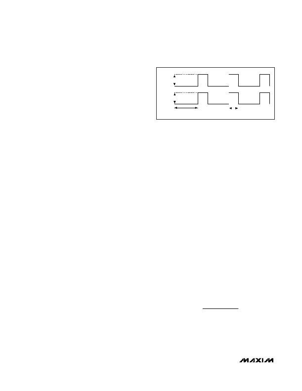
�Figure� 5.� Blink� Timer� Behavior�
�Both� comparators� reset� at� a� fixed� time� after� the� rising�
�edge� of� the� second� comparator� trip� point,� generating� a�
�minimum� width� pulse� t� ON(MIN)� at� the� output� of� the� sec-�
�ond� comparator.� As� the� input� voltage� increases� or�
�decreases,� the� duration� of� the� pulse� at� one� output�
�increases� (the� first� comparator� to� trip),� while� the� other�
�output� pulse� duration� remains� at� t� ON(MIN)� .� This� causes�
�the� net� voltage� across� the� speaker� (SPK+� -� SPK-)�
�to� change.�
�Adjustable� Differential� Gain�
�The� audio� amplifier� has� an� internal� gain� control.� The�
�gain� of� the� input� amplifiers� is� controlled� through� the� I� 2� C�
�interface.� The� gain� setting� of� the� input� amplifier� can� be�
�set� from� -3dB� to� +24dB� (Table� 15).� This� allows� the�
�amplifier� to� be� used� for� both� hands-free� and� for� receiv-�
�er� mode� without� any� external� components.�
�Input� Filter�
�The� fully� differential� amplifier� inputs� can� be� biased� at�
�voltages� other� than� midsupply.� The� common-mode�
�feedback� circuit� adjusts� for� input� bias,� ensuring� the�
�outputs� are� still� biased� at� midsupply.� Input� capacitors�
�are� not� required� as� long� as� the� common-mode� input�
�voltage� is� within� the� specified� range� listed� in� the�
�Electrical� Characteristics� table.� If� input� capacitors� are�
�used,� input� capacitor� C� IN� ,� in� conjunction� with� on-chip�
�R� INT� ,� forms� a� highpass� filter� that� removes� the� DC� bias�
�from� an� incoming� signal.� The� AC-coupling� capacitor�
�allows� the� amplifier� to� bias� the� signal� to� an� optimum� DC�
�level.� Assuming� zero-source� impedance,� the� -3dB� point�
�of� the� highpass� filter� is� given� by:�
�device� remains� disabled� for� a� minimum� of� 110μs� before�
�attempting� to� return� to� normal� operation.� The� amplifier�
�shuts� down� immediately� and� waits� another� 110μs� before�
�f� ?� 3� dB� =�
�1�
�2� ×� π� ×� R� INT� ×� C� IN�
�turning� on� if� the� fault� condition� remains.� This� operation�
�causes� the� output� to� pulse� during� a� persistent� fault.�
�Comparators� monitor� the� MAX8821� inputs� and� compare�
�the� complementary� input� voltages� to� the� sawtooth� wave-�
�form.� The� comparators� trip� when� the� input� magnitude� of�
�the� sawtooth� exceeds� their� corresponding� input� voltage.�
�Setting� the� -3dB� corner� too� high� affects� the� low-fre-�
�quency� response� of� the� amplifier.� Use� capacitors� with�
�dielectrics� that� have� low-voltage� coefficients,� such� as�
�aluminum� electrolytic.� Capacitors� with� high� voltage�
�coefficients,� such� as� ceramics,� can� increase� distortion�
�at� low� frequencies.�
�18�
�______________________________________________________________________________________�
�发布紧急采购,3分钟左右您将得到回复。
相关PDF资料
MAX8822ETE+T
IC LED DRVR WHITE BCKLGT 16-TQFN
MAX8830EWE+T
IC LED DRVR WHITE BCKLGT 16-UCSP
MAX8831EWE+T
IC LED DRIVR WHITE BCKLGT 16-WLP
MAX8834ZEWP+T
IC LED DRIVR BCKLGT FLASH 20-WLP
MAX8855EVKIT+
KIT EVAL FOR MAX8855
MAX8879ETG+T
IC LED DRVR WT/RGB BCKLGT 24TQFN
MAX8901BETA+TCH8
IC LED DRIVER WHITE BCKLGT 8TDFN
MAX8930EWJ+T
IC LED DRVR WT/RGB BCKLGT 49WLP
相关代理商/技术参数
MAX8821ETI+T
功能描述:LED照明驱动器 White LED Charge Pump RoHS:否 制造商:STMicroelectronics 输入电压:11.5 V to 23 V 工作频率: 最大电源电流:1.7 mA 输出电流: 最大工作温度: 安装风格:SMD/SMT 封装 / 箱体:SO-16N
MAX8821EVKIT+
功能描述:电源管理IC开发工具 MAX8821 Eval Kit RoHS:否 制造商:Maxim Integrated 产品:Evaluation Kits 类型:Battery Management 工具用于评估:MAX17710GB 输入电压: 输出电压:1.8 V
MAX8822ETE+
功能描述:LED照明驱动器 Negative Charge Pump LED Driver RoHS:否 制造商:STMicroelectronics 输入电压:11.5 V to 23 V 工作频率: 最大电源电流:1.7 mA 输出电流: 最大工作温度: 安装风格:SMD/SMT 封装 / 箱体:SO-16N
MAX8822ETE+T
功能描述:LED照明驱动器 Negative Charge Pump LED Driver RoHS:否 制造商:STMicroelectronics 输入电压:11.5 V to 23 V 工作频率: 最大电源电流:1.7 mA 输出电流: 最大工作温度: 安装风格:SMD/SMT 封装 / 箱体:SO-16N
MAX882C/D
功能描述:低压差稳压器 - LDO RoHS:否 制造商:Texas Instruments 最大输入电压:36 V 输出电压:1.4 V to 20.5 V 回动电压(最大值):307 mV 输出电流:1 A 负载调节:0.3 % 输出端数量: 输出类型:Fixed 最大工作温度:+ 125 C 安装风格:SMD/SMT 封装 / 箱体:VQFN-20
MAX882C/D DIE
制造商:Maxim Integrated Products 功能描述:
MAX882CPA
功能描述:低压差稳压器 - LDO 5/3.3/AdjV 200mA Linear Regulator RoHS:否 制造商:Texas Instruments 最大输入电压:36 V 输出电压:1.4 V to 20.5 V 回动电压(最大值):307 mV 输出电流:1 A 负载调节:0.3 % 输出端数量: 输出类型:Fixed 最大工作温度:+ 125 C 安装风格:SMD/SMT 封装 / 箱体:VQFN-20
MAX882CPA+
功能描述:低压差稳压器 - LDO 5/3.3/AdjV 200mA Linear Regulator RoHS:否 制造商:Texas Instruments 最大输入电压:36 V 输出电压:1.4 V to 20.5 V 回动电压(最大值):307 mV 输出电流:1 A 负载调节:0.3 % 输出端数量: 输出类型:Fixed 最大工作温度:+ 125 C 安装风格:SMD/SMT 封装 / 箱体:VQFN-20